Motor Control
Chapter 2
Single Phase Induction Motor Control
Table of Contents
2.1 Hardware required
2.2 Connection Procedure
2.3 PWM generation to run the Single Phase Induction Motor
This section discuss about the PWM generation to control the single phase induction motor.
2.1 Hardware required
1. RIO – cRIO 9054
a. Slot 1: NI 9220
b. Slot 3: NI 9401
c. Slot 4: NI 9401
2. 3 Leg Inverter with measurements
3. 1 HP Single phase induction motor.
2.2 Connection procedure
1. Using auto transformer, connect the three phase AC supply to the AC input of converter.
2. Connect the Multimeter in the DC Voltage mode across the Capacitor voltage terminals (DC + and DC -)
3. Connect R Phase and Y phase output of the conveter to Phase and Neutral of the single phase induction motor.
4. RIO hardware connection
(a) Mod 4 / DIO 0 – Pin 14 – H1 Pulse input
(b) Mod 4 / DIO 1 – Pin 16 – L1 Pulse input
(c) Mod 4 / DIO 2 – Pin 17 – H2 Pulse input
(d) Mod 4 / DIO 3 – Pin 19 – L2 Pulse input
(e) Mod 4 / COM – Pin 13 – Pulse Ground
2.3 PWM generation to run the Single Phase Induction Motor
1. Open the New FPGA VI under the FPGA Target.
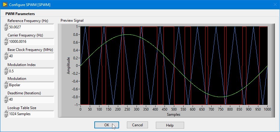
2. Select Function Palette > PE libraries for FPGA > PWM > SPWM and add it in to the block diagram. Configure the SPWM Express VI as given below.
(a) Reference Frequency (Hz) : 50
(b) Carrier Frequency (Hz): 10,000
(c) Base Clock Frequency (MHz): 40
(d) Modulation Index: 0.5
(e) Modulation: Bipolar
(f) Deadtime (Iterations): 40
(g) Lookup Table Size: 1024 Samples.
3. Select Function Palette > PE Libraries for FPGA > Time > Loop time in ticks and connect it to the loop time in ticks input of SPWM node.

4. Create the controls of the Reset, Enable PWM, Reference Frequency (periods/ticks), Carrier Frequency (periods/ticks), Modulation Index and Deadtime (iterations).

5. Set the Mod 4 (NI 9401) DIO channels line direction as output. (Refer 2.2.1).
6. Add the Mod 4 / DIO 0, DIO3 to the block diagram and connect it to the High Pulse. Add the Mod 4 /DIO1 and DIO 2 to the block diagram and connect it to the Low pulse.

7. Create the While loop to run the program continuously.

Block diagram of the SPWM for Single phase Induction motor FPGA VI- Quick Run

Front panel of the SPWM for single phase induction motor FPGA VI
8. Save the FPGA VI (SPWM_QR_Bipolar.vi) and Click the run button to compile the FPGA VI.
9. Create the New VI in the RT Target.
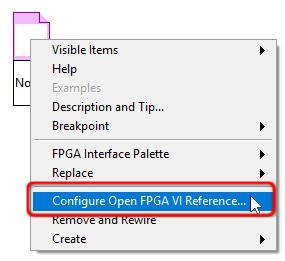
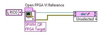
10. Select Function Palette > FPGA Interface > Open FPGA VI Reference and add it to the block diagram. Right click on node and select the Configure Open FPGA VI Reference.
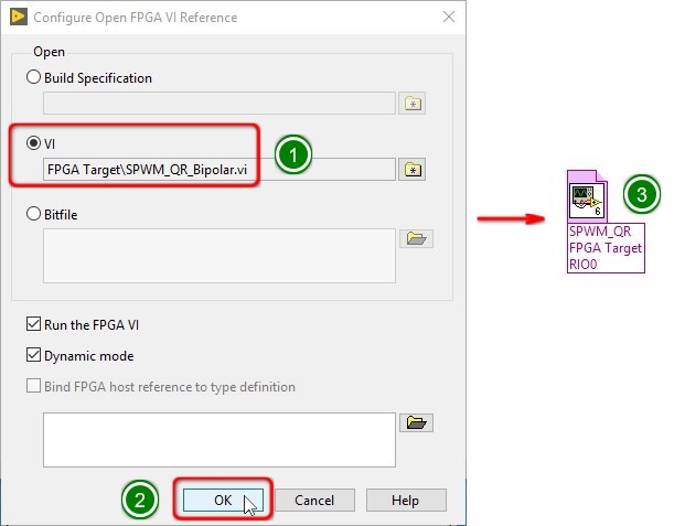
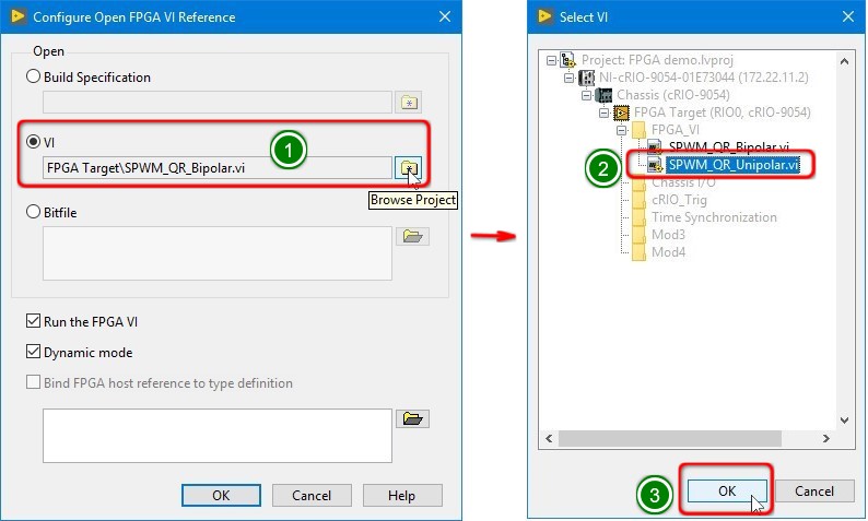
11. Select the VI (1) based FPGA VI call and select the FPGA VI (2) saved in step 8. Click the OK button (3)

12. Confirm the FPGA VI (1) selected and Click OK button (2). The Open FPGA VI Reference node is configured to use the FPGA VI saved in the step 8.
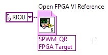
13. Add constant to the FPGA Resource Name input of the Open FPGA VI Reference node and select RIO0
14. Add Read / Write Control (Function Palette > FPGA Interface > Read / Write Control) to the block diagram and connect the FPGA VI Reference and Error out from Open FPGA VI reference to Read/Write Control Node.
15. Click the unselected property of the Read/Write Node and select it as Reference Frequency (periods/ticks). Expand it to access all the variables available in the FPGA VI.

16. Add the Close FPGA VI Reference (Function Palette > FPGA Interface > Close FPGA VI Reference) to the block diagram and connect it to the Read/Write Control node.

17. By default, the divide node provides the output as doubt data type. Configure the divide node output as fixed-point data type, 32 Bit word length and 0 bit for integer word length.
18. Add the While loop to the read/write node with its controls & indicator. Add the Wait function (100ms delay) to the while loop.
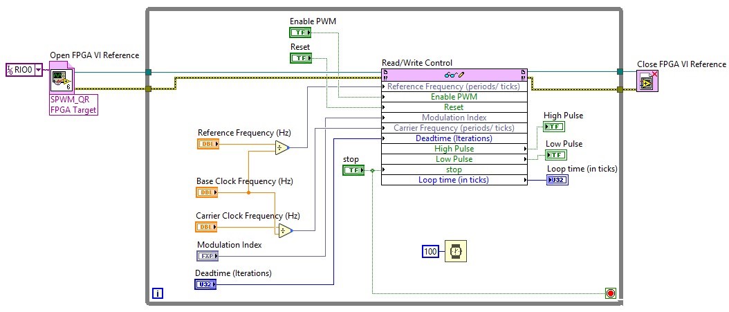
Block diagram of the SPWM for single phase induction motor RT VI
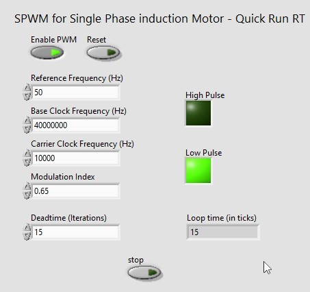
Front panel of the SPWM for Single Phase Induction motor RT VI
19. Save the VI in the name as RT_SPWM_QR_Bipolar.vi
20. Click the Run button in the RT VI front panel.It will load the FPGA VI in the FPGA target and execute it. We can give the input values through the RT VI. RT VI runs at 10Hz (1/100ms) for user interface. The FPGA VI Runs at 2.66MHz (one iteration takes 15 ticks at 40MHz clock).
21. The recommended dead time for this inverter is 5µs.
(a) Dead time (in iterations) = dead time in seconds / (loop time in ticks x 1/ base clock)
(b) Dead time (in iterations) = 0.000005 / (15 x 1/40M) = 0.000005 / 0.000000375 = 13.33
(c) Dead time (in iterations) = 14 iterations.
22. Update the dead time in the RT VI.
23. Observe the top and bottom PWM Pulses of each leg in the oscilloscope. Make sure that top and bottom pulses are having dead time between them. 
SPWM Pulses of the single phase inverter (leg one top and bottom pulses)
24. Turn on the power supply to the Inverter kit.
25. Slowly increase input AC voltage using autotransformer. And set the DC bus voltage as 220VDC
26. Vary the modulation index and reference sine waveform frequency. The induction motor speed will vary with respect to the reference sine waveform frequency.
27. Take the required reading and tabulate it.
28. Reduce the 3 Phase AC power supply to 0V and turn off power supply to the inverter.
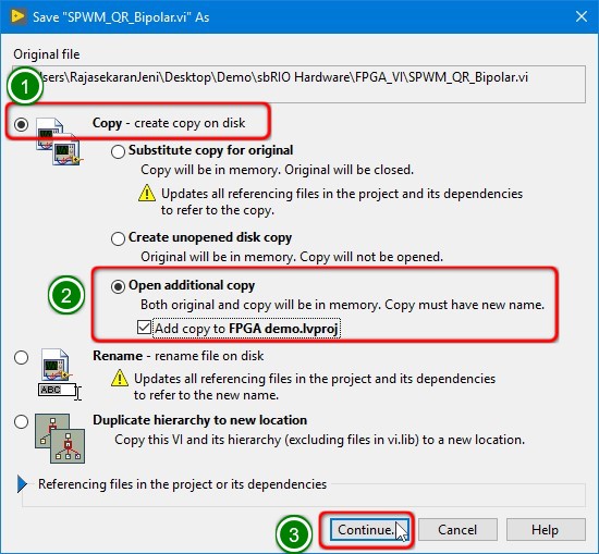
29. Open the SPWM_QR_Bipolar FPGA VI and select File > Save as. Select Copy (1) > Open additional Copy and select Add Copy to FPGA demo.lvproj (2) . Click Continue button (3).
30. Save the file as SPWM_Unipolar.vi.
31. Double click the SPWM Express VI to open the configuration window. Change the Modulation from Bipolar to Unipolar-I (1). And click OK button (2).

32. Click the Run button to compile the FPGA VI.
33. Open the RT_SPWM_QR_Bipolar and make the copy as RT_SPWM_QR_Unipolar.vi
34. Open the RT_SPWM_QR_Unipolar VI. Right click on the Open FPGA VI Reference and select Configure Open FPGA VI Reference.
35. Select the VI browse (1) option and Select the SPWM_QR_Unipolar VI (2) and Click the OK (3) Button.
36. Confirm the SPWM_QR_Unipolar VI (1) and click the OK (2) button. Now the Open FPGA VI Reference (3) will load the new SPWM_QR_Unipolar VI (3).

37. Run the RT_SPWM_QR_Unipolar RT VI.
38. The SPWM Unipolar FPGA VI takes 19 ticks to complete one iteration. The revised deadtime for the SPWM pulse is 10.52 iterations. Update the deadtime as 12 iterations.

39. Observe the top and bottom pulses of each leg in the oscilloscope.Make sure that top and bottom pulses are having dead time between them.
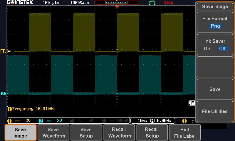
SPWM Pulses for single phase inverter – Unipolar (leg one – top and bottom pulses)

SPWM Pulses for single phase inverter – Unipolar (leg one – top and bottom pulses) (zoomed view)
40. Repeat the steps from 24-28 and repeat the speed control of the induction motor in the Unipolar SPWM pulses.
