Motor Control
Chapter 6
PMSM Motor Control
Table of Contents
6.1 Hardware required
6.2 Connection procedure
6.3 PWM generation to run the PMSM Motor
6.1 Hardware required
- RIO – cRIO 9054
- Slot 1: NI 9220
- Slot 3: NI 9401
- Slot 4: NI 9401
- 3 Leg Inverter with measurements
- 1 HP PMSM Motor with Hall sensor
6.2 Connection procedure
- Using auto transformer, connect the three phase AC Supply to the AC input of the converter.
- Connect the Multimeter in the DC Voltage mode across the Capacitor Voltage terminals (DC+ and DC-)
- Connect the Converter output R, Y and B Terminals to Phase A, Phase B and Phase C power supply terminals of the PMSM motor.
- RIO Hardware Connection
- Mod 4 / DIO 0 – Pin 14 – H1 Pulse input
- Mod 4 / DIO 1 – Pin 16 – L1 Pulse input
- Mod 4 / DIO 2 – Pin 17 – H2 Pulse input
- Mod 4 / DIO 3 – Pin 19 – L2 Pulse input
- Mod 4 / DIO 4 – Pin 20 – H3 Pulse input
- Mod 4 / DIO 5 – Pin 21 – L3 Pulse input
- Mod 4 / COM – Pin 13 – Pulse Ground
- Mod 3 / DIO 0 – Pin 14 –Hall A
- Mod 3 / DIO 1 – Pin 16 – Hall B
- Mod 3 / DIO 2 – Pin 17 – Hall C
- Mod 3 / DIO 7 – Pin 25 – Hall 5V input
- Mod 3 / COM – Pin 13 – Hall Ground
- Connect 2.2kΩ / 0.25W Resistor between Hall A and Hall 5V terminal
- Connect 2.2kΩ / 0.25W Resistor between Hall B and Hall 5V terminal.
- Connect 2.2kΩ / 0.25W Resistor between Hall C and Hall 5V terminal.
6.3 PWM generation to run the PMSM Motor
1. Open the New VI under FPGA Target
2. Select Function Palette > PE Libraries for FPGA > PWM > PMSM Motor to the block diagram and configure it as given below.
(a) Carrier Frequency (Hz): 10,000
(b) Base Clock Frequency (MHz): 40
(c) Duty Cycle: 0.5
(d) Lookup Table Size: 1024 Samples

3. Select Function Palette > PE Libraries for FPGA > Time > Loop time in ticks and connect it to the loop time input of the PMSM Motor Express VI.

4. Set DIO Module line direction (refer 2.2.1)
(a) Mod 3: DIO 0-3: Input
(b) Mod 3: DIO 4-7: Output
(c) Mod 4: DIO 0-3: Output
(d) Mod 4: DIO 4-7: Output
5. Add Mod3 / DIO0, Mod3 / DIO 1 and Mod 3 /DIO 2 to the Hall A, Hall B and Hall C Respectively.

6. Create the controls for the Reset, Enable PWM, Frequency (Periods/ticks) and Duty Cycle and indicators for H1, L1, H2, L2, H3 and L3.

7. Add the Mod4 DIO lines 0,1,2,3,4 and 5 to the block diagram and connect it to H1, L1, H2, L2, H3 and L3 respectively.

8. Create the While loop to run the program continuously.

9. Select Function Palette > PE Libraries for FPGA > Time > Speed and add it to the block diagram. Connect the Mod3/ DIO0 to the pulse input. Create constants for the Base Clock, Pulse per revolution and Cycles to Filter.
(a) Base Clock: FPGA Base clock frequency
(b) Pulse per revolution: Number of pulses generated by hall sensor per revolution. The rotor having 12 poles and it will generate 5 pulses per revolution.
(c) Cycles to Filter: Number of Clock cycles to filter the noise signal in the proximity input. If noise signals are present in the hall sensor feedback, increase the value gradually up to 100 cycles.

10. Create the While loop for the speed measurement VI.

11. Right Click on the Boolean Stop button (1) available in the While loop created in step 7 and select Create > Local Variable (2) . Place Local Variable in the speed measurement loop (3).

12. Right Click on the Local Variable (1) and select Change to Read (2). Connect the Stop Local variable output to the stop condition of the speed measurement loop (3).

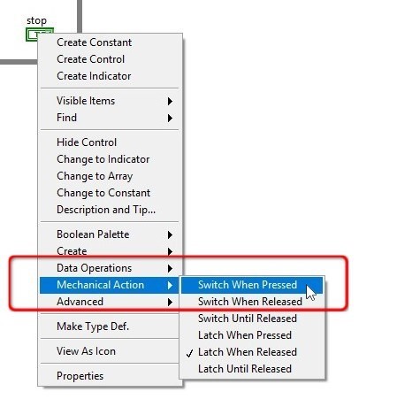
13. Right Click on the Boolean Stop (in the PWM Loop) button and Select Mechanical Action > Switch When pressed.
14. Add the Mod3/DIO 7 to Speed measurement loop and set it as Digital output. Connect Boolean Constant True to the Mod3/DIO 7 output. It is used to give 5V output to the Hall Sensor.

15. Save the FPGA VI (PMSM Quick Run.VI) and click the Run button to compile it.
16. Create a New VI in the RT Target.
17. Select Function Palette > FPGA Interface > Open FPGA VI Reference and add it to the block diagram. Right click on the node and select Configure Open FPGA VI Reference.
18. Select the VI based FPGA VI Call and Select the FPGA VI Saved in step 15 (1). Click OK button (2) to select the file. Again click the OK button save the configuration. Add constant to the FPGA Resource input of the Open FPGA VI Reference and Select RIO0 (3).

19. Add Read / Write Control (Function Palette > FPGA Interface > Read / Write Control) to the block diagram and connect the FPGA VI Reference In and Error In 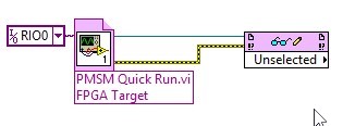
20. Left Click on the Unselected and create the Controls and Indicators to access the variables available in the FPGA VI.

21. Add the Close FPGA VI Reference (Function Palette > FPGA Interface > Close FPGA VI Interface) to the block diagram and connect the FPGA VI Reference In and Error In.

22. Add the While loop to the read/write node with its controls & indicator. Add the Wait function (100ms delay) to the while loop.

Block diagram of the RT VI for PMSM Motor Control

Front Panel of the RT VI for PMSM Motor Control
23. Save the RT VI in the name as RT_PMSM_Motor_Control.vi and Run it.
24. Manually rotate the PMSM motor shaft and ensure that all the three hall sensor feedbacks are measured, and we are getting the all the six commutation states.
25. Turn on the power supply to the Inverter Kit.
26. Slowly increase the three phase AC Supply using auto transformer and set the DC bus voltage as 48V.
27. Click the Enable PWM button to set it as True.
28. Slowly increase the duty cycle and observe the motor speed. The PMSM motor speed will vary with respect to the Duty Cycle.
29. Take the necessary readings by varying the duty cycle.
30. Reduce the AC power supply to 0V using auto transformer.
31. Turn off the power supply to the inverter kit.
32. Stop the program.
